Employee Spotlight: Gavyn Trowbridge

Ionoptika is very proud of its skilled and dedicated staff, who together with our loyal users make up our global community. In our ongoing series, we shine the spotlight on one of our talented colleagues each month to introduce you to some of the people behind Ionoptika.

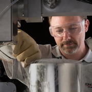
This month we move away from new hires to what will be a very familiar face to many of our customers around the world, Senior Test & Service Engineer, Gavyn Trowbridge. Gavyn is one of Ionoptika’s longest serving employees, joining the company in 2004, and today he manages our customer installations and service work around the world. We asked Gavyn for an insight into his time at Ionoptika.

"...knowing that the whole team has had a part to play in the completion of the project, and knowing I am inserting the final piece of the puzzle, whilst installing it, brings a certain joy that can't be explained" - Gavyn Trowbridge, Senior Test & Service Engineer

How long have you worked at Ionoptika and what career path brought you to us?

I joined Ionoptika in Feb 2004, having previously worked in various roles in the manufacturing sector including a PCB factory, high power micro generators, up to 100kW of power from gas turbines. I self-educated through night school and day release. The role at Ionoptika suited me because I have always been interested in taking things apart, seeing how they work, and putting them back together.

What do you enjoy most about working at Ionoptika?

I appreciate the diverse range of skills and experience we have in the factory team, and the toys are pretty cool too. We get paid to play with toys!!

But the prospect that we may be creating something that could change the world for the better is a real buzz; a pharmaceutical breakthrough? A medical research breakthrough? New things never seen before in the field?

You never know what research, or researchers you may meet in the field on a customer site. The projects that our customers work on are each fascinating in their own way!

My favourite part of the role is the final installation of the instruments: knowing that the whole team has had a part to play in the completion of the project, and knowing I am inserting the final piece of the puzzle, whilst installing it, brings a certain joy that can’t be explained.

Can you describe a typical day working at Ionoptika (normally, not in the lockdown!)

There’s never a dull moment in my day and no such thing as a typical day. One day I may be building a prototype, another fixing something, and another testing a customer system. Or just general helping of others with my long-term experience?  I also usually spend quite a lot of time on customer sites around the world.

What has been your best memory or achievement during your time at Ionoptika?

The installation of the J105 instruments is quite exciting. You never know where one might be going and it’s a real buzz to travel to global customer sites to install these systems.

What do you enjoy doing in your spare time?

Gaming, music, walking, meditation, the great outdoors. Often meditating in places of beauty.

Have you been doing anything interesting/different/new to cope with the lockdown?

Trying to stay sane!!! Making the most of not being away and making home improvements.

What are you looking forward to most once the lockdown is over?

Enjoying the great outdoors more, exploring new places. This year’s holiday was going to be an eastern European adventure, taking in 4 countries, but this is now postponed until next year!


Interested in becoming part of our team? Visit our Careers page.

GCIB-SEM: 3D electron microscopy with < 10nm isotropic resolution

GCIB-SEM is a new technique that combines high resolution electron microscopy with the damage free sputtering of gas cluster ions to produce incredible 3D tomography with less than 10 nm isotropic resolution.

Over the last two decades, gas cluster ion beams (GCIB) have become increasingly popular as add-on components for ultra-high vacuum techniques such as XPS, SPM, and SIMS. Due to their excellent combination of fast yet low-damage sputtering, GCIBs have been widely adopted as depth profiling ion beams, or as a means of cleaning samples in situ.

Very low impact energies, as little as 1 eV per atom, means cluster ions sputter material without modifying the surface chemistry, i.e. without breaking bonds. This makes GCIBs particularly effective for high-resolution depth profiling of soft materials such as polymers and organic matter.

GCIB 10S cluster schematic, and PET C 1s XPS spectrum comparing Ar1 and Ar2000.
The GCIB 10S is a powerful tool for damage-free depth profiling of polymers, organics, and other soft materials, delivering consistently superior results over monatomic beams.

Traditional sputter beams such as Ar1 typically have impact energies in the kilovolt range, resulting in not only large amounts of fragmentation to surface molecules, but also penetration of the ions beneath the surface causing further damage. This damage shows up in XPS and SIMS spectra, and limits the depth resolution of the technique.

Cluster beams also sputter soft, organic material much faster than hard, inorganic materials, making them extremely useful for removing adventitious carbon and other surface contamination without damaging the substrate — ideal for cleaning surfaces prior to analysis.

It is no surprise then that GCIBs have become so popular as add-on components for surface analysis instrumentation.

The GCIB 10S

  • 10 kV argon cluster ion source
  • Selectable clusters from Ar1 to > Ar3000
  • Real-time cluster measurement & adjustment
  • Sample current imaging
  • Gate valve for quick & easy servicing
  • Large spot size and wide scan field for even removal of material

The versatile nature of the GCIB makes it a useful tool in a variety of other techniques as well, beyond strictly surface science. In particular, the GCIB has recently been shown to be powerful tool in electron microscopy. A new technique pioneered by researchers at HHMI Janelia Research Campus combines high resolution electron microscopy with the damage free sputtering of gas cluster ions to produce incredible 3D tomography with less than 10 nm isotropic resolution.

Published in Nature Methods in 2019 the GCIB-SEM system developed by Hayworth et al. consists of a GCIB 10S from Ionoptika mounted on a Zeiss Ultra SEM. Using 1 µm thick serial sections of brain tissue, high-resolution electron imaging was interleaved with wide-area ion milling until the entire section was consumed. Full experimental details can be found in the paper linked above.

Figure detailing results achieved using GCIB SEM, by Hayworth et al
GCIB-SEM is a powerful technique for acquiring extremely detailed 3D maps on an unprecedented scale. Images from a GCIB-SEM run performed on three sequential 500-nm-thick sections of mouse cortex. bioRxiv: http://dx.doi.org/10.1101/563239.

The result is a 3D data set hundreds of microns in area by tens of microns deep, with less than 10 nm isotropic resolution throughout. Such a high resolution data set then allows researchers to map the brain structure in incredible detail. The figure above shows a 15 x 15 x 10 µm section of mouse brain, the detail of which is truly remarkable. Panel e shows a single spiney dentritic process with axons synapsing on it, while panel f shows various high-resolution 2D and 3D views of a single spiney synapse.

Other technologies used to perform similar experiments include FIB-SEM and diamond knife based sectioning, however both have their drawbacks. FIB provides the necessary resolution, but is thus far incompatible with the high-throughput needed for larger volumes, while diamond knife techniques are highly compatible with larger volumes, but lack the consistency needed at such thin cuts.

In contrast, the GCIB 10S mills away just the top few nanometres of the surface resulting in an improvement in depth resolution of a factor of 3 or more over other techniques, whilst simultaneously improving sectioning reliability. The rapid, wide area milling afforded by the GCIB 10S is also compatible with the new multi-beam SEM systems now on the market, which will enable even larger volumes to be analysed with no loss of resolution.

GCIB-SEM

  • Large-area and fast (up to 450 µm3 s-1).
  • Can be automated and is highly scalable.
  • Consistent performance over large volumes.
  • Simple, easy to maintain, and reliable.
  • Improves z resolution by a factor of 3 or more.

GCIB-SEM is a powerful technique for exploring complex materials and structures in three dimensions with extraordinary detail. For this application, control of the cluster size and current is critical to the result. Unlike other gas cluster beams, the GCIB 10S lets the user take complete control of the experiment. With real-time cluster measurement, cluster size can be tuned to the users’ needs and the settings saved for later use.

Real-time cluster measurement on the GCIB 10S

The GCIB 10S is easily installed on a range of instrumentation, from XPS and SIMS, to electron microscopes, Auger, and more. To speak with us and find out how the GCIB 10S might be right for your application, or to request a brochure, please get in touch via our Contact Page.