 Ionoptika 2020
What is Ion Implantation?
Ion implantation is a process whereby dopant ions are accelerated in intense electrical fields to penetrate the surface of a material, thus changing the material’s properties.
An essential technique in the semiconductor industry, it is used for modifying the conductivity of a semiconductor during the fabrication of integrated circuits. It is also heavily used for making silicon-on-insulator devices and in many other industries, including physics, materials science, and metallurgy.
Virtually all ion implantation applications involve implanting vast numbers of ions over a large area to modify the bulk properties of a material. In contrast, Q-One is designed for implanting single ions with extremely high precision to fabricate quantum devices. However, many of the same concepts apply.
Ion Implanters
Ion implanters consist of a source region that forms the ions, an accelerator region that electrostatically accelerates them to high energy, and a target chamber. Instruments must be pumped to a high vacuum to prevent contamination of the target and breakdown under high voltage.
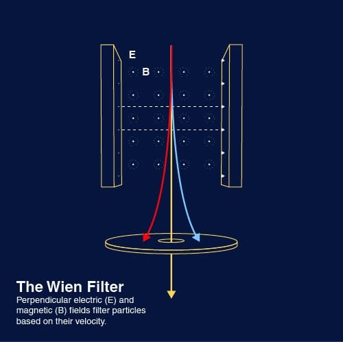
Ion sources often generate multiple ions depending on design, including different elements, their isotopes, and multiple charge states for each. A magnetic filter, also known as a Wien filter, is often used to select specific ions based on their velocity.
The implanting species, also called dopants, vary considerably with the application. Boron, arsenic and phosphorous are the most common dopants in semiconductor applications, while oxygen and nitrogen are used to process metals. Dopants for quantum applications include phosphorous,1 nitrogen,2–5 silicon,6–8 and germanium,9, and rare earth elements such as erbium.10
Implanters are often categorised by the ion beam current at the target, either low, medium or high. High-current systems for commercial applications operate at up to tens of milliamps and process hundreds of wafers per hour. On the other hand, Q-One operates at extremely low currents when implanting single ions, often tens of femtoamps.11
The ion dose is the integral of the ion current per unit area over time, measured in ions per square centimetre (ions/cm2). The dose determines the concentration of the dopant in the target. Common dose values are in the range 1016 – 1018 ions/cm2.
Beam Energy & Ion Stopping
The energy of the ion beam is a crucial parameter in ion implantation processes as it has several significant effects. The energy is the product of the accelerator voltage and the ion’s charge state, measured in electron volts (eV). For example, a Bi2+ ion accelerated in a 30 kV field has an energy of 60 keV.
Ions hitting a target lose their kinetic energy through collisions with the nuclei and electrons of the material until they stop. The depth to which the ions penetrate depends on their energy and mass, the target mass, and the beam’s angle to the crystal plane in the case of a single crystal. Higher energies penetrate further for a given mass, while lighter elements penetrate further than heavy elements for a given energy.12
The energy range of ion implantation instruments can range from 1 keV to several MeV. Q-One operates in the range of 5 – 30 kV, with an option to extend this to 40 kV. In this range, the ions penetrate approximately 5 – 100 nm beneath the surface – suitable for most quantum applications.
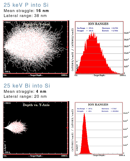
As the ions stop, they become laterally displaced from their initial trajectory, known as straggle. Straggle is an important consideration when it comes to single-ion implantation. The precision with which ions are positioned is the sum of the beam diameter at the target plus the lateral straggle. In some instances, the straggle is much larger than the beam and, therefore, the limiting factor.
Straggle is proportional to the energy and inversely proportional to the mass. So lowering the implantation energy and selecting heavier elements results in greater precision by reducing the straggle.
Damage
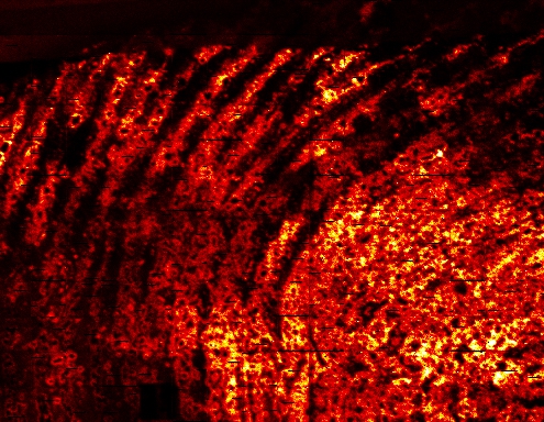
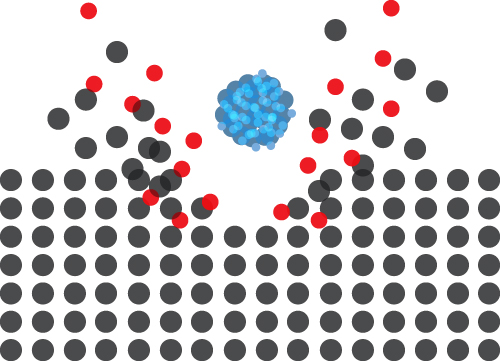
Ion implantation is a violent process. The projectile transfers a large amount of its kinetic energy to the target atoms, displacing them from the lattice sites. The primary collisions result in secondary collisions, and so on, in a process known as collision cascade.
The collision cascade forms a variety of defects in the material, including vacancies, interstitials, amorphous zones, stacking faults, and dislocation loops, among others.12 Thermal annealing post-implantation restores the crystalline order and allows the device to function. High temperatures can also cause diffusion of the implanted atoms, so annealing steps must be designed carefully.
Sputter Yield
The beam energy also has an important effect on the sputter yield. Ions impinging on a surface do not just penetrate the surface. They also sputter material, which is an important consideration, particularly at low energy.
The sputter yield (Y) is the mean number of atoms removed from the target surface per incident ion. If Y > 1, the ions remove more target material per implanted ion, resulting in erosion. If Y < 1, the ions sputter fewer target atoms per implanted ion, and material builds up. When Y = 1, there is a one-for-one replacement of target atoms with implanted ions.
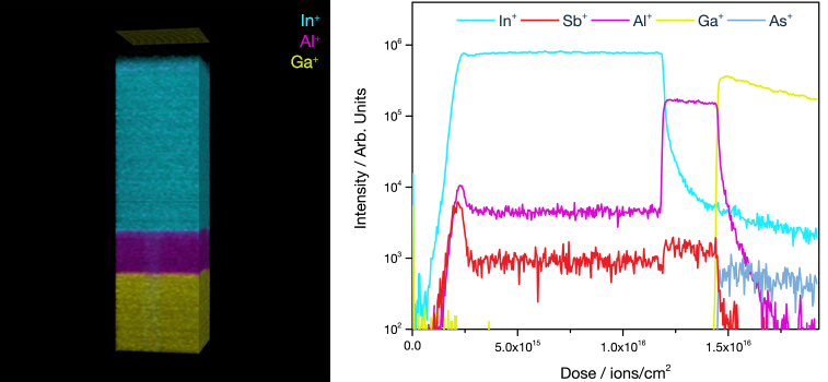
Holmes et al. use TRIDYN simulations to model the sputter yield of 28Si impinging natural silicon at various energies.6 They show that the three regimes are energy-dependent and that Y = 1 at two energies, 3 and 45 keV, resulting in a planar surface. However, operating at 45 keV produces a much deeper implant and is thus more suitable for device fabrication.
Want to know more about Q-One and how it can impact your research? Get in touch with our team today, and we’d be happy to help.
References
- Morello, A. et al. Single-shot readout of an electron spin in silicon. Nat. 2010 4677316 467, 687–691 (2010) https://doi.org/10.1038/nature09392.
- Gruber, A. et al. Scanning confocal optical microscopy and magnetic resonance on single defect centers. Science (80-. ). 276, 2012 (1997) https://doi.org/10.1126/science.276.5321.2012.
- Naydenov, B. et al. Increasing the coherence time of single electron spins in diamond by high temperature annealing. Appl. Phys. Lett. 97, 242511 (2010) https://doi.org/10.1063/1.3527975.
- Brouri, R., Beveratos, A., Poizat, J.-P. & Grangier, P. Photon antibunching in the fluorescence of individual color centers in diamond. Opt. Lett. 25, 1294 (2000) https://doi.org/10.1364/OL.25.001294.
- Mizuochi, N. et al. Electrically driven single photon source at room temperature in diamond. Nat. Photon. 6, 299 (2012) https://doi.org/10.1038/nphoton.2012.75.
- Holmes, D. et al. Isotopic enrichment of silicon by high fluence 28Si- ion implantation. Phys. Rev. Mater. 5, 014601 (2021) https://doi.org/10.1103/PhysRevMaterials.5.014601.
- Wang, C., Kurtsiefer, C., Weinfurter, H. & Burchard, B. Single photon emission from SiV centres in diamond produced by ion implantation. J. Phys. B At. Mol. Opt. Phys. 39, 37 (2006) https://doi.org/10.1088/0953-4075/39/1/005.
- Neu, E. et al. Single photon emission from silicon-vacancy colour centres in chemical vapour deposition nano-diamonds on iridium. New J. Phys. 13, 025012 (2011) https://doi.org/10.1088/1367-2630/13/2/025012.
- Iwasaki, T. et al. Germanium-Vacancy Single Color Centers in Diamond. Sci. Reports 2015 51 5, 1–7 (2015) https://doi.org/10.1038/srep12882.
- Yin, C. et al. Optical addressing of an individual erbium ion in silicon. Nat. 2013 4977447 497, 91–94 (2013) https://doi.org/10.1038/nature12081.
- Cassidy, N. et al. Single Ion Implantation of Bismuth. Phys. status solidi 218, 2000237 (2021) https://doi.org/10.1002/pssa.202000237.
- Rimini, E. Ion Implantation: Basics to Device Fabrication. Ion Implant. Basics to Device Fabr. (1995) https://doi.org/10.1007/978-1-4615-2259-1.
- Ziegler, J. F., Ziegler, M. D. & Biersack, J. P. SRIM – The stopping and range of ions in matter (2010). Nucl. Instruments Methods Phys. Res. Sect. B Beam Interact. with Mater. Atoms 268, 1818–1823 (2010) https://doi.org/10.1016/j.nimb.2010.02.091.

 Ionoptika
 ionoptika
 Ionoptika 2020
 Ionoptika
 ionoptika
 Ionoptika Ltd
 Ionoptika Ltd
 Ionoptika 2020
 Ionoptika 2020
 Ionoptika Ltd
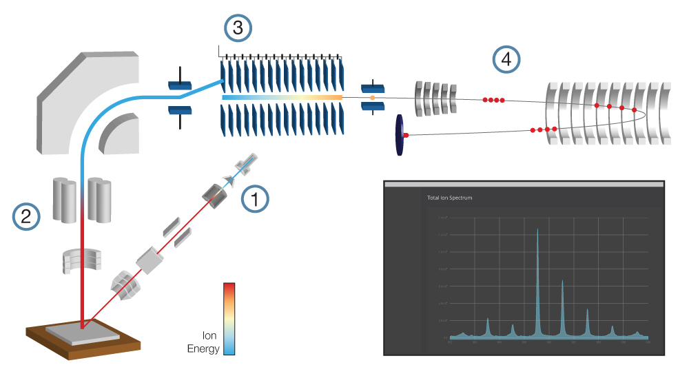

 Ionoptika Ltd
 Ionoptika 2020
 Ionoptika 2020
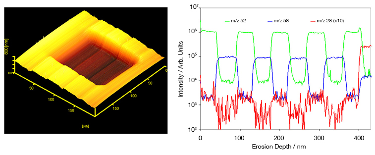

 Ionoptika Ltd 2020